Looking from front to back,
the output board runs the length of the back panel, except for the
far left side where the power supply board lives.
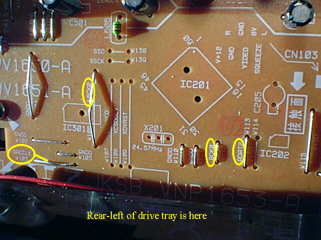
Immediately behind the drive tray you can find 4 jumpers
which carry:
Note that these jumpers are simply convenient test locations. It's possible that cleaner signals can be obtained nearer the IC901, 904, 906 Clock Generator chips, which are on the DVDM (green) controller board.
The digital audio outputs are on the far right of the output board. The same signal goes to the coaxial digital output (electrical) and optical, each passing in series through their own pair of 74HCT04 inverter gates before reaching their output connections. (The outputs are therefore non-inverting relative to their input.) The coax digital out is further buffered in that the second inverter stage is actually three inverter gates connected in parallel for better drive.
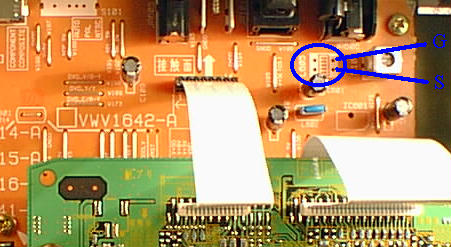
Tracing out the bottom, the S/PDIF signal appears at
one position of a missing transformer. That hole, towards the front of
the chassis, has a pointer "S" for signal.
On the same (right) side of the missing coil, but towards the back,
is a signal ground marked "G":
However, the S/PDIF signal at the missing
tranformer holes seems to run about 1 V p-p.
Instead we should be able to tap the 5 V version of the signal
at the left pin of coil L602, which is fed directly from the
'04 inverter.
Or it may be desireable to pick up the separately buffered
copy of the signal that goes to the Toslink output
(or whichever digital output ends up not used).